\(I_{V1} + \frac{v_{1}}{R_{1}} - \frac{v_{2}}{R_{1}} = 0\)
\(I_{L1} + v_{2} \left(C_{2} s + \frac{1}{R_{1}}\right) - \frac{v_{1}}{R_{1}} = 0\)
\(C_{1} s v_{3} - I_{L1} = 0\)
\(v_{1} = V_{1}\)
\(- I_{L1} L_{1} s + v_{2} - v_{3} = 0\)
3 Modified Nodal Analysis
In 1975, Ho, Ruehli, and Brennan (1975) published a paper titled, The Modified Nodal Approach to Network Analysis. This was the original scholarly paper on the subject. The analysis method they presented allows for the ability to process voltage sources and current-dependent circuit elements in a simple and efficient manner. The paper describes the formulation of the matrices, the use of stamps and a pivot ordering strategy. The authors compare their algorithm to the tableau method, a circuit analysis technique, which was an analysis technique being described in scholarly papers at the time. At the time of this publication, the authors were affiliated with the IBM Thomas J. Watson Research Center in Yorktown Heights, N.Y.
The development of MNA was driven by the critical need for efficient circuit equation formulation in computer-aided design programs, particularly for integrated circuits. While the traditional nodal approach offered flexibility and efficiency for manual analysis, its inherent limitations—especially concerning the treatment of voltage sources and current-dependent elements—demanded a more generalized and computationally friendly method. This highlights a pattern of industry-driven innovation; the practical demands of integrated circuit design within a leading industrial research center directly spurred this fundamental analytical advancement.
The timing of MNA’s publication in 1975 was opportune, coinciding with the maturation of digital computing capabilities, which enabled its rapid and widespread adoption as the computational infrastructure became ready to fully leverage its algorithmic advantages. If MNA had been proposed much earlier, the computational resources might not have been sufficient to efficiently handle the large matrices generated. By 1975, digital computers had advanced to a point where MNA’s sophisticated matrix operations and iterative solutions became practically feasible and efficient. This technological readiness allowed MNA’s inherent algorithmic advantages to be fully exploited, leading to its rapid integration into circuit simulation software and its eventual dominance.
Circuit analysis and theory are fundamental to electrical engineering and is usually one of the first topics taught to electrical engineering students. The purpose of this book is to describe a circuit analysis method called Modified Nodal Analysis (MNA) implemented in Python and using the SymPy library.
Consider the example circuit shown in Figure 3.1. This circuit has five branches and three nodes. There is a voltage source \(V_1\), which drives the circuit and each of the nodes is labeled along with the ground node.
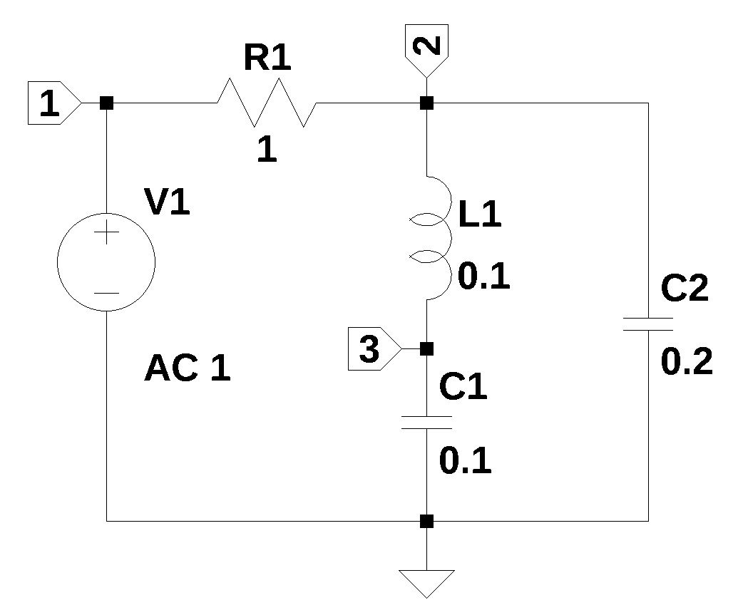
For this circuit, the MNA procedure generates the following system of equations:
Test output
\(C_{1} s v_{1} - C_{1} s v_{2} + I_{L1} + I_{V1} = 0\)
\(- C_{1} s v_{1} + v_{2} \\left(C_{1} s + \\frac{1}{R_{1}}\\right) - \\frac{v_{4}}{R_{1}} = 0\)
\(- I_{L1} + \\frac{v_{3}}{R_{2}} - \\frac{v_{5}}{R_{2}} = 0\)
\(I_{V2} - \\frac{v_{2}}{R_{1}} + \\frac{v_{4}}{R_{1}} = 0\)
\(I_{F1} - \\frac{v_{3}}{R_{2}} + \\frac{v_{5}}{R_{2}} = 0\)
\(v_{4} = V_{2}\)
\(v_{1} = V_{1}\)
\(- I_{L1} L_{1} s + v_{1} - v_{3} = 0\)
\(I_{F1} - I_{V2} f_{1} = 0\)
where, \(s\) is the Laplace variable, \(C_1\) and \(C_2\) are capacitors, \(R_1\) is a resistor, \(L_1\) is an inductor, \(v_1\), \(v_2\) and \(v_3\) are the unknown node voltages, \(V_1\) is the input voltage source, \(I_{V1}\) is the unknown current flowing through \(V_1\) and \(I_{L1}\) is the unknown current flowing in \(L_1\).
The first of theses five equations is the KVL equation for node 1, where current through \(R_1\) is equal to the current from \(V_1\). The second equation describes the current flowing from branches connected to node 2. For node 2, the unknown current in \(L_1\) is assigned to \(I_{L1}\). The third equation describes the current flowing from the branches into node 3. The fourth equations just says that the voltage at node 2 is equal to \(V_1\). The last equation describes the current in \(L_1\). There are five network equations in total, but one of the equations, \(v_1=V_1\) is trivial.
Solving this set of equations is easily accomplished by using a computer with MATLAB, Python with NumPy, an on-line matrix calculator or a modern graphical calculator that has matrix algebra capabilities. Inverting a 4 by 4 matrix by hand is probably the largest matrix that would be attempted given the numerous modern calculating tools available.
These equations can be solved by the afore mentioned tools to obtain the unknown voltages and currents as either numerical or analytic expressions. The analytical expression for the unknown voltages and currents are displayed below.
\(v_{1} = V_{1}\)
\(v_{2} = \frac{C_{1} L_{1} V_{1} s^{2} + V_{1}}{C_{1} C_{2} L_{1} R_{1} s^{3} + C_{1} L_{1} s^{2} + C_{1} R_{1} s + C_{2} R_{1} s + 1}\)
\(v_{3} = \frac{V_{1}}{C_{1} C_{2} L_{1} R_{1} s^{3} + C_{1} L_{1} s^{2} + C_{1} R_{1} s + C_{2} R_{1} s + 1}\)
\(I_{V1} = \frac{- C_{1} C_{2} L_{1} V_{1} s^{3} - C_{1} V_{1} s - C_{2} V_{1} s}{C_{1} C_{2} L_{1} R_{1} s^{3} + C_{1} L_{1} s^{2} + C_{1} R_{1} s + C_{2} R_{1} s + 1}\)
\(I_{L1} = \frac{C_{1} V_{1} s}{C_{1} C_{2} L_{1} R_{1} s^{3} + C_{1} L_{1} s^{2} + C_{1} R_{1} s + C_{2} R_{1} s + 1}\)
In the following chapters, Python will be used to automatically generate and solve circuit analysis problems using Python, SymPy, NumPy and SciPy.
3.1 Pros and Cons of MNA
The MNA approach is a suitable technique for hand analysis of small circuits as well as for computer analysis of larger circuits using the same algorithm as illustrated in this book. One disadvantage of the MNA technique is that often additional equations are generated, when a smaller number would be sufficient. For students doing homework problems and solving sets of equations by hand, the extra equation or two, generated by the MNA technique makes matrix inversions much harder.
For example, the circuit in Figure 3.1, can be described by the following two mesh equations:
\(\displaystyle L_{1} s \left(i_{1} - i_{2}\right) + R_{1} i_{1} + \frac{i_{1} - i_{2}}{C_{1} s} = V_{1}\)
\(\displaystyle L_{1} s \left(- i_{1} + i_{2}\right) + \frac{i_{2}}{C_{2} s} + \frac{- i_{1} + i_{2}}{C_{1} s} = 0\)
where \(i_1\) and \(i_2\) are the unknown currents.
The MNA procedure generated five equations (but one of them was trivial) to find the node voltages, whereas only two equations are need to be solved to find the mesh currents, which are:
\(i_{1} = \frac{C_{1} C_{2} L_{1} V_{1} s^{3} + C_{1} V_{1} s + C_{2} V_{1} s}{C_{1} C_{2} L_{1} R_{1} s^{3} + C_{1} L_{1} s^{2} + C_{1} R_{1} s + C_{2} R_{1} s + 1}\)
\(i_{2} = \frac{C_{1} C_{2} L_{1} V_{1} s^{3} + C_{2} V_{1} s}{C_{1} C_{2} L_{1} R_{1} s^{3} + C_{1} L_{1} s^{2} + C_{1} R_{1} s + C_{2} R_{1} s + 1}\)
Modern pocket scientific calculators that engineering students now use can solve sets of linear equations relatively easily. However, some effort is required to enter the equations into the calculator.
When a computer is used to generate the schematic for a circuit and the net list is exported to the Python code, the extra equations that the MNA approach generates is not a practical concern. Using the examples in this book as templates for problem solving makes the work flow very easy, which is the main benefit of using MNA.
3.2 Formulation of the Modified Nodal Equations
Modified nodal analysis provides an algorithmic method for generating systems of independent equations for linear circuit analysis. The systematic application of MNA can be broken down into a series of procedural steps, ensuring a consistent approach to equation formulation:
- Node Definition and Reference Node Selection: The process begins by identifying all distinct nodes within the circuit. A crucial first step is to select a reference node, typically designated as ground.
- Assign Unknowns: Unique variable names are assigned to all unknown node voltages. Additionally, variables are assigned to represent the unknown currents flowing through independent voltage sources, inductors or current-dependent sources.
- Apply KCL at Nodes: For each non-reference node with an unknown voltage, a Kirchhoff’s Current Law (KCL) equation is written for each branch. When a voltage source is connected to a node, the current through that voltage source is treated as an explicit unknown variable within the KCL equation for the connected nodes.
- Formulate System of Equations: Combine all the KCL equations and the voltage source unknowns into a system of algebraic equations.
- Solve the System of Equations: The complete linear system of equations can then be efficiently solved using matrix methods to determine all unknown node voltages and the specified branch currents.
As describe below, the outline procedure above is implement in terms of matrices and “element stamps”.
The “element stamp” concept is a fundamental enabler of MNA’s algorithmic efficiency, modularity and its widespread adoption as the core of modern circuit simulation software. This approach means that instead of a simulator needing to derive KCL equations for every node, it can simply iterate through each component in the circuit’s netlist.
For each component, the pre-defined “stamp” - a small matrix/vector contribution – is directly inserted into the corresponding location in the global MNA matrix. This modular, additive approach drastically simplifies the algorithm for building the system matrix, making it highly efficient, less prone to errors and easily extensible to new component models.
3.2.1 Matrix Formulation
The MNA procedure formulates the entire set of circuit equations into a system of linear algebraic equations represented in matrix form: \(A \cdot X=Z\).
where \(A\) is System Matrix, \(X\) is vector containing the Unknowns and \(Z\) is a vector containing the Knowns.
This matrix representation is fundamental to its computational efficiency and scalability, providing a structured approach for solving complex circuit problems.
For circuits containing reactive elements such as capacitors and inductors, the initial MNA formulation can results in a system of Differential Algebraic Equations (DAEs) or Ordinary Differential Equations (ODEs). But in this book, the Laplace variable \(s\) is used.
3.2.2 Detailed Structure of the System Matrix
The system matrix, is a square matrix with dimensions of (n+m) by (n+m). Where, ‘n’ denotes the number of nodes in the circuit (excluding the ground reference node), and ‘m’ represents the number of independent voltage sources. This matrix is populated with known quantities derived directly from the circuit’s passive elements and source interconnections.
Conceptually, the A matrix is partitioned into four distinct sub-matrices, each contributing to specific aspects of the circuit’s behavior:
Matrix \(A\) describes the connectivity of the resistors, capacitors and G type (VCCS) circuit elements. The \(X\) vector contains unknown node voltages and unknown currents from the voltage sources and inductors. The \(Z\) vector contains the known voltages and currents. The \(A\) matrix is formed by four sub matrices, \(G\), \(B\), \(C\) and \(D\), which are described below.
\[A = \begin{bmatrix}G B\\C D\end{bmatrix} \tag{3.1}\]
The matrix \(G\) is formed from the coefficients representing the KCL equations for each node. The positive diagonal of \(G_{k,k}\) are the conductance terms of the resistor and capacitor elements connected to node k. The off diagonal terms of \(G_{k,j}\) are the resistors and capacitor conductances connecting node k to node j. G type elements (VCCS) have input to the G matrix at the connection and controlling node positions.
The \(B\) matrix describes the connectivity of the unknown branch currents. Independent voltage sources, Op Amps, H, F and E type elements as well as inductors have inputs to the B matrix.
The \(C\) matrix describes the connectivity of the unknown branch currents and is mainly the transpose of the \(B\) matrix, with the exception of the F type elements (CCCS) and includes the E type value.
The \(D\) matrix also describes connectivity of the unknown currents. The \(D\) matrix is composed of zeros unless there are controlled sources and inductors in the network.
The \(X\) vector is composed of the \(V\) and \(J\) vectors as shown in Equation 3.2.
\[X = \begin{bmatrix}V\\J\end{bmatrix} \tag{3.2}\]
The \(V\) vector contains the node voltages which are the voltage unknowns to be solved for. The \(J\) vector contains the unknown currents from each voltage source.
The \(Z\) vector is composed of the I and Ev vectors as shown Equation 3.3.
\[Z = \begin{bmatrix}I\\Ev\end{bmatrix} \tag{3.3}\]
The I vector contains the known currents and the Ev vector contains the known voltages. The name Ev is used because SymPy uses e and E sometimes for the constant 2.71, also called Euler’s number. The use of E or e as a symbol was causing some errors when the code was run.
Putting all the parts together:
\[\begin{bmatrix}G B\\C D\end{bmatrix} \cdot \begin{bmatrix}V\\J\end{bmatrix} = \begin{bmatrix}I\\Ev\end{bmatrix} \tag{3.4}\]
3.2.2.1 Stamps
Stamps are templates for modifying the terms of Equation 3.4. The stamps follow the circuit connections of the components to directly populate the matrices. See Section 4.7 through Section 4.14 for discriptions and the Python code used to stamp the matrices and build the network equations.
3.3 Python Code Description
The Python code that implements the MNA procedure is divided in the following sections.
Preprocessor: The preprocessor reads in the netlist text file and removes comments, extra spaces and blank lines. The first letter of the element type is capitalized to make subsequent parsing of the file easier. The number of lines are counted and the number of entries on each line are checked to make sure the count is consistent with the element type.
Parser: The parser code loads the preprocessed netlist into a data frame. A report is generated which consists of a count of the element types in the netlist.
Matrix formulation: The matrices and vectors of Equation 3.4 are generated.
Circuit equation generation: The circuit equations are generated by the SymPy code:
NE_sym = Eq(A*Matrix(X),Matrix(Z))
in Section 4.18. SymPy automatically does some simplification according to its default settings.
3.4 Netlist file format
The input file which describes the circuit is a text file called the netlist. A netlist consists of a statement defining each circuit element and its connection to circuit nodes. A node is any point on a circuit where two or more circuit elements meet. The nodes are numbered from 1 to N in any order and node 0 is the ground node or circuit common. A ground node is required. Choose a ground or reference node, which usually is taken to be at a potential of zero volts. All other node voltages constitute n unknowns. The nodes should be numbered in consecutive order. Each line in the netlist are either comments, SPICE directives or circuit elements.
SPICE directives are commands to SPICE and the first character on the line is a period. Comment lines start with a * or ;. The default file extension is ‘.net’. The Python code does some preprocessing of the netlist to check the basic formatting of the netlist is correct.
The preprocessor performs the following steps:
- remove blank lines and comments
- convert first letter of element name to uppercase
- removes extra spaces between entries
- counts number of entries on each line to make sure the count is correct and counts each element type
The element types that are supported are resistors, capacitors, inductors, independent sources and controlled sources. Each line in the netlist file contains a circuit element.
The format for the element description is
letterXX n1 n2 value
Where
letter signifies the element type, i.e. R, L, C, V, I, O, E, F, G, H or K
XX is a string of letters or numbers that uniquely identify the element.
The element types are described in the following sections.
3.4.1 Resistors, capacitors and inductors
The resistors, capacitors and inductors are described by the following line:
R/L/CXX N1 N2 value
Where:
XX = the name of the component, can be any length
N1 = the first terminal
N2 = the second terminal
Value = component value in ohms, Farads or Henrys.
For example, a resistor named R1 connected between nodes 1 and 2 with a value of 3000 ohms.
R1 2 4 3000
SPICE supports other parameters, but these are not allowed in this Python implementation.
3.4.2 Coupled inductors
Two coupled inductors are described by the following line.
KXX LYY LZZ VALUE
The parameters are:
LYY = the name of the first coupled inductor
LZZ = the name of the second coupled inductor
VALUE = the coefficient of coupling, K, where \(-1 \lt k \lt 1\)
The orientation of the inductors is determined by the first node, which is considered to be the dotted node. When LTSpice generates a net list the phasing dot gets associated with the negative node. This does not seem to affect the equations generated by the Python code. LTSpice uses the coupling coefficient, \(k\). The symbolic equations use the mutual inductance, \(M\) as shown in Equation 3.5.
\[M = k\sqrt{L_1L_2} \tag{3.5}\]
See Chapter 9 and Chapter 35 for example circuits that have coupled inductors and the code to calculate \(M\) and substitute a numerical value into the symbolic network equations.
The ideal transformer is a losses unity coupled transformer and is defined by the turns ratio, \(n=\frac{N_2}{N_1}\), where \(N_1\) and \(N_2\) are the numbers of turns on the primary and secondary coils. The following relationship holds:
\[\frac {L_2}{L_1} = \Biggl ( \frac{N_2}{N_1} \Biggr ) ^2 = n^2 \tag{3.6}\]
In circuits where only the turns ratio of the transformer is given, an equivalent circuit is usually used. One such equivalent circuit is a voltage controlled voltage source with a gain of \(V_2/n\) used on the primary side and a current controlled current source with a gain of \(i_1/n\) is used for the secondary side.
3.4.3 Independent sources
Independent sources are formatted as if they are DC sources, even if the source is intended to be an AC source. The value of the source or its type, AC or DC, doesn’t matter when seeking a symbolic solution. The numeric value of the source can be changed when doing a numerical analysis, by following the procedures illustrated in the test or problem circuits. A voltage source is described by the following line.
VXX N+ N- VALUE
The parameters are:
N+ = the name of the positive terminal
N- = the name of the negative terminal
VALUE = the value of the DC voltage
A current source is described by the following line.
IXX N+ N- VALUE
The parameters are:
N+= the name of the positive terminal, current leaves this terminal (pointy end of the arrow)
N- = the name of the negative terminal
VALUE = the value of the DC current
3.4.4 Controlled sources
The voltage-controlled dependent sources are defined using statements of the form
GXX or EXX nout+ nout- nc+ nc- gain
where E is a voltage-controlled voltage source, G is a voltage-controlled current source, the output voltage is connected between nodes nout+ and nout-, and the control voltage is measured at node nc+ with respect to node nc-.
Examples:
E1 5 1 4 3 10 defines a voltage source that makes node 5 a voltage 10 times (v4 - v3) above the voltage at node 1.
G1 2 1 5 8 50 defines a current source connected between node 2 (the + node) and node 1 and supplying a current 50 times (v5 - v8).
The current-controlled dependent sources are defined by statements of the form
FXX or HXX nout+ nout- Vcontrol gain
where F is a current-controlled current source, H is a current-controlled voltage source, and the output current source is connected between nodes nout+ and nout-, with positive current flowing through the source from node nout+ to nout-. The control current flows from the positive node of the source Vcontrol through the source and out the negative node.
Examples:
F1 11 9 Vsens 1.25 defines a current source connected from node 11 to node 9 that generates a current 1.25 times the current flowing through the source Vsens.
H1 30 20 V5 100 defines a voltage source connected from node 30 to node 20 and supplying a voltage 100 times the current through the source V5. It is frequently necessary to add a voltage source with value 0 V to the circuit to sense the control current for these sources.
The direction of positive controlling current flow is from the positive node, through the source, to the negative node of VNAM. VALUE is the current gain. The symbols used for the gains of the dependent sources are: \(ea_n\), \(g_n\), \(f_n\) and \(h_n\). Note that the symbolic gain for a voltage controlled voltage source is \(ea_n\) and not a single letter as is used for the other controlled source types. The symbol \(e\) is already used in SymPy for the mathematical constant, Euler’s number, \(e=2.718\).
3.4.5 Op Amps
An Op Amp component is described by the following line.
OXX N+ N- Vout
The output of the Op Amp is a voltage source.
The Op Amp element is assumed to be an ideal Op Amp and the voltage at the input terminals are defined by the model to equal each other. The use of this component is valid only when used in a network with a path from the output terminal to the negative input terminal of the Op Amp. No error checking is provided and if the condition is violated, the results will be likely erroneous. Op Amp circuits with Inductors and/or capacitors in the feedback path may not analyze correctly at \(s = 0\) or \(s = \infty\). See Chapter 21 and Chapter 22 for additional comments.
3.4.6 Nullor, Gyrator and others
There are other circuit elements that are sometimes discussed in text books and technical papers, amoung these are: Nullors, Gyrators, Negative Impedance Converters (NIC), Frequency-Dependent Negative Resistors (FDNR) and Memristors. Follow the links to read more about these element types. The table below summarizes these components:
| Element | Key Relationship | Primary Function |
|---|---|---|
| Gyrator | \(V \leftrightarrow I\) | e.g. transforms \(C \rightarrow L\) |
| Nullor | \(V_{in}=0 \text{, } I_{in}=0\) | Models an ideal Op-Amp |
| NIC | \(Z \rightarrow -Z\) | Produces negative resistance or capacitance |
| FDNR | \(1/s^2\) | Used to replace inductors with capacitors in filters |
| Memristor | \(\Phi \leftrightarrow q\) | Memory-based resistance |
At this time, the theoretical elemets in Table 3.1 have not been implememted in the Python code presented in this book. With a little work, element stamps for these components could be incorperated into the Python code. However, except for the Memristor, it is possile to emulate the function of these components with the circuit elements currently defined in the Python code.
3.5 Analysis procedure
- Draw the circuit to be analyzed in LTSpice or some other schematic capture program. Label the nodes. The Symbolic Modified Network Analysis code will provide warnings for netlist formatting errors and non consecutive node numbering, but will still generate nodal equations which may be erroneous. Users should verify the results.
- Export the netlist of the circuit and convert component values to units of Ohms, Farads and Henrys. Use scientific notation, for example, replace component values such as 2k with 2e3 and 2u with 2e-6.
- Change Op Amp reference designators, for example U1 to O1 (capitol letter O, not zero).
- Voltage sources and current sources need to be set to zero in some cases. See test circuits and problem circuits for examples.
- Call the
smna(net_list)function. - See the example problem and verification test chapters for examples on how to use Python and MNA for symbolic and numerical circuit analysis. Use the JupyterLab notebooks as templates.
3.6 Summary
Modified Nodal Analysis stands as a pivotal and enduring cornerstone of modern electrical engineering. It represents a significant evolution from classical nodal analysis, meticulously designed to overcome its critical limitations, particularly concerning the efficient representation of ideal voltage sources and current-dependent elements. MNA’s systematic matrix formulation (Ax=z) and the ingenious concept of “element stamps” fundamentally transformed circuit analysis from a laborious manual task into a highly efficient, algorithmically driven process. This transformation was directly catalyzed by the burgeoning field of computer-aided design, which demanded more robust and scalable analytical tools.
Invented by Chung-Wen Ho, Albert E. Ruehli, and Pierce A. Brennan in 1975 at IBM Research, MNA’s impact was immediate and profound. Its development at a leading industrial research institution underscores its origins as a pragmatic solution to real-world challenges in integrated circuit design, highlighting the critical role of corporate innovation in advancing fundamental engineering methodologies. The timing of its publication was also crucial, coinciding with the maturation of digital computing capabilities, which allowed its algorithmic advantages to be fully leveraged, leading to its rapid and widespread adoption.
MNA swiftly became the underlying computational engine for virtually all commercial circuit simulators, most notably the ubiquitous SPICE family (e.g., LTspice, JSpice). This powerful method enables a comprehensive suite of essential circuit analyses, including DC operating point, AC frequency response, transient time-domain behavior, and noise analysis, while also supporting advanced applications such as symbolic model generation. Its ability to serve as a unifying mathematical framework across these diverse analysis types streamlines the architecture of complex simulation software, enhancing its versatility and power.
While historically experiencing a period of under representation in some academic curricula, MNA is now increasingly recognized as an indispensable pedagogical tool. Its integration into electrical engineering education is crucial for bridging the gap between theoretical circuit concepts and the practical realities of computer-aided design, preparing students for the demands of the modern industry. Furthermore, ongoing research continues to refine MNA’s numerical properties and explore its applications to emerging challenges and new device technologies, ensuring its sustained vitality and relevance. MNA is not merely an analytical method; it is a foundational framework that underpins the design, verification, and innovation of virtually all contemporary electronic systems.